Showing posts with label Power Supply. Show all posts
WEARIFY

Reliable Car Battery Tester Circuit Diagram

Reliable Car Battery Tester Circuit Diagram

This circuit uses the popular and easy to find LM3914 IC. This IC is very simple to drive, needs no voltage regulators (it has a built in voltage regulator) and can be powered from almost every source. This circuit is very easy to explain: When the test button is pressed, the Car battery voltage is feed into a high impedance voltage divider. His purpose is to divide 12V to 1,25V (or lower values to lower values).

This solution is better than letting the internal voltage regulator set the 12V sample voltage to be feed into the internal voltage divider simply because it cannot regulate 12V when the voltage drops lower (linear regulators only step down). Simply wiring with no adjust, the regulator provides stable 1,25V which is fed into the precision internal resistor cascade to generate sample voltages for the internal comparators. Anyway the default setting let you to measure voltages between 8 and 12V but you can measure even from 0V to 12V setting the offset trimmer to 0 (but i think that under 9 volt your car would not start).

There is a smoothing capacitor (4700uF 16V) it is used to adsorb EMF noise produced from the ignition coil if you are measuring the battery during the engine working. Diesel engines would not need it, but I'm not sure. If you like more a point graph rather than a bar graph simply disconnect pin 9 on the IC (MODE) from power. The calculations are simple (default)

For the first comparator the voltage is : 0,833 V corresponding to 8 V
* * * * * voltage is : 0,875 V corresponding to 8,4 V
for the last comparator the voltage is : 1,25 V corresponding to 12 V
Have fun, learn and don't let you car battery discharge... ;-)
Read More
WEARIFY

Glass Break Alarm Circuit Diagram

This circuit can be used for sounding an alarm to detect the breaking of a glass window by an intruder, even when the intruder ensures there is no sound of the shattered glass.
Fig. 1: Circuit of the glass break alarm

Circuit and working
  
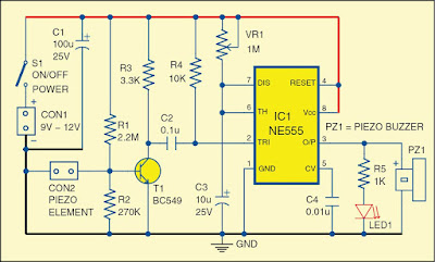
Fig. 1 shows the circuit diagram of the glass break alarm. It is built around a piezo element connected across connector CON2, transistor BC549 (T1), timer NE555 (IC1), a piezo buzzer (PZ1) and a few other components.
A small piezo element used in the piezo buzzer is used as a sensor. It may be fixed at the centre of the window glass. IC1 is wired in monostable multivibrator mode, which is triggered by the piezo element. Output of IC1 is used to drive piezo buzzer PZ1. LED1 indicates the high-state output at pin 3 of IC1. Time delay can be adjusted by potentiometer VR1. Use an ordinary piezo buzzer at the output to generate a warning sound. This circuit works on 9V-12V DC.

When an intruder tries to break the glass, the piezo element generates an electric pulse, which is amplified and sent to the monostable multi-vibrator (IC1). The high output of IC1 drives LED1 and also produces a sound to indicate that someone is breaking the glass.

The 9V-12V DC power supply is connected across CON1, and the piezo element is connected across connector CON2.

Construction and testing
An actual-size, single-side PCB for the glass break alarm is shown in Fig. 2 and its component layout in Fig. 3. Enclose the PCB in a suitable small box in such a way that the piezo buzzer sounds when someone tries to break the glass window. Fix the piezo element at the centre of the window glass for best results.

Fig. 2: Actual-size PCB of the glass break alarm

Fig. 3: Component layout of the PCB


Use of 8-pin IC base is recommended for IC NE555.
Read More
WEARIFY

A Handy Pen Torch Circuit Diagram

This easy to construct “Handy pen torch” electronic circuit and low component count, uses two power white LEDs for lighting. Low volt (4.8V dc) supply available from the built in rechargeable Ni-Cd battery pack is first converted into two channel (independent) constant current sources by two pieces of the renowned precision adjustable shunt regulator chip LM334 (IC1 and IC2). Around 25mA at 3.6 volt dc is available at the output of these ICs.

This regulated dc supply is used to drive two power white LEDs D4 and D6. Resistors R3 and R5 limits the output current (and hence the light output) of IC1 and IC2 circuits respectively. Besides these components, one red color LED (D2) is included in the main circuit which works as a battery charging supply input indicator. Resistor R1 limits the operating current of this LED.

Pen Torch Electronic Circuit Schematic

A Handy Pen Torch Circuit Diagram


Diode D1 works as an input polarity guard cum reverse current flow preventer. Capacitor C1 is a simple buffer for circuit stabilization. After succesful construction, preferably on a small piece of general purpose PCB, enclose the whole circuit in a suitable and attractive pen torch cabinet. If necessary, drill suitable holes in the cabinet to attatch the dc socket, on/off switch and the input indicator etc. In prototype,commonly available 4.8 volt/500mah Ni-Cd battery pack (for cordless telephones) is used.

One very simple but reliable ac mains powered battery charger circuit for the handy pen torch is also included here. Basically the pen torch circuit is a constant current charger wired around Transistor T1 (BC636), powered by a 12v/350mA step down transformer and associated componentsD1, D2 and C1.

AC mains powered battery charger for the pen torch


A Handy Pen Torch Circuit Diagram
Unregulated 12 volt dc available from the input power convereter circuit, comprising step down transformer(TRF), rectifier diodes (D1,D2) and filter capacitor (C1), is fed to T1 through a current limiting resistor R1. Grounded base PNP transistor T1 here works as a constant current generator. With 22 ohm resistor for R1, the charging current available at the output of the charger is near 50mA.

Red LED (D3) provides a fixed voltage reference to the base of T1, with the help of resistor R2. (During charging process, Diode D1 in the main circuit prevent reverse current flow from the battery pack when charging input supply is absent.) After construction of the pen torch circuit, fit the assembled unit inside a small plastic enclosure for safety and convenience.
Read More
WEARIFY

Solar Powered SLA Battery Maintenance Schematic

This circuit was designed to ‘baby-sit’ SLA (sealed lead-acid or ‘gel’) batteries using freely available solar power. SLA batteries suffer from relatively high internal energy loss which is not normally a problem until you go on holidays and disconnect them from their trickle current charger. In some cases, the absence of trickle charging current may cause SLA batteries to go completely flat within a few weeks. The circuit shown here is intended to prevent this from happening. Two 3-volt solar panels, each shunted by a diode to bypass them when no electricity is generated, power a MAX762 step-up voltage converter IC.

Solar Powered SLA Battery Maintenance Circuit Diagram:

Solar Powered SLA Battery Maintenance Schematic

The ‘762 is the 15-volt-out version of the perhaps more familiar MAX761 (12 V out) and is used here to boost 6 V to 15 V.C1 and C2 are decoupling capacitors that suppress high and low frequency spurious components produced by the switch-mode regulator IC. Using Schottky diode D3, energy is stored in inductor L1 in the form of a magnetic field. When pin 7 of IC1 is open-circuited by the internal switching signal, the stored energy is diverted to the 15-volt output of the circuit. The V+ (sense) input of the MAX762, pin 8, is used to maintain the output voltage at 15 V. C4 and C5 serve to keep the ripple on the output voltage as small as possible. R1, LED D4 and pushbutton S1 allow you to check the presence of the 15-V output voltage.

D5 and D6 reduce the 15-volts to about 13.6 V which is a frequently quoted nominal standby trickle charging voltage for SLA batteries. This corresponds well with the IC’s maximum, internally limited, output current of about 120 mA. The value of inductor L1 is not critical — 22 µH or 47 µH will also work fine. The coil has to be rated at 1 A though in view of the peak current through it. The switching frequency is about 300 kHz. A suggestion for a practical coil is type M from the WEPD series supplied by Würth (www.we-online.com). Remarkably, Würth supply one-off inductors to individual customers. At the time of writing, it was possible, under certain conditions, to obtain samples, or order small quantities, of the MAX762 IC through the Maxim website at www.maxim-ic.com.
Read More
WEARIFY

TRANSFORMERLESS 5 VOLT DC POWER SUPPLY

An increasing number of appliances draw a very small current from the power supply. If you need to design a mains-powered device, you could generally choose between a linear and a switch-mode power supply. However, what if the appliance’s total power consumption is very small? Transformer-based power supplies are bulky, while the switchers are generally made to provide greater current output, with a significant increase in complexity, problems involving PCB layout and, inherently, reduced reliability.

Is it possible to create a simple, minimum part-count mains (230 VAC primary) power supply, without transformers or coils, capable of delivering about 100mA at, say, 5 V? A general approach could be to employ a highly inefficient stabilizer that would rectify AC and, utilizing a zener diode to provide a 5.1 V output, dissipate all the excess from 5.1 V to (230×√2) volts in a resistor. Even if the load would require only about 10mA, the loss would be approximately 3 watts, so a significant heat dissipation would occur even for such a small power consumption.


Transformerless 5 Volt DC Power Supply Circuit Diagram:

TRANSFORMERLESS 5 VOLT DC POWER SUPPLY

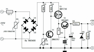
At 100mA, the useless dissipation would go over 30 W, making this scheme completely unacceptable. Power conversion efficiency is not a major consideration here; instead, the basic problem is how to reduce heavy dissipation and protect the components from burning out. The circuit shown here is one of the simplest ways to achieve the above goals in practice. A JVR varistor is used for over-voltage/surge protection. Voltage divider R1-R2 follows the rectified 230 V and, when it is high enough, T1 turns on and T3 cannot conduct.

When the rectified voltage drops, T1 turns off and T3 starts to conduct current into the reservoir capacitor C1. The interception point (the moment when T1 turns off) is set by P1 (usually set to about 3k3), which controls the total output current capacity of the power supply: reducing P1 makes T1 react later, stopping T3 later, so more current is supplied, but with increased heat dissipation. Components T2, R3 and C2 form a typical ‘soft start’ circuit to reduce current spikes — this is necessary in order to limit C1’s charging current when the power supply is initially turned on. At a given setting of P1, the output current through R5 is constant.

Thus, load R4 takes as much current as it requires, while the rest goes through a zener diode, D5. Knowing the maximum current drawn by the load allows adjusting P1 to such a value as to provide a total current through R5 just 5 to 6mA over the maximum required by the load. In this way, unnecessary dissipation is much reduced, with zener stabilization function preserved. Zener diode D5 also protects C1 from over voltages, thus enabling te use of low-cost 16 V electrolytics. The current flow through R5 and D5, even when the load is disconnected, prevents T3’s gate-source voltage from rising too much and causing damage to device. In addition, T1 need not be a high-voltage transistor, but its current gain should exceed 120 (e.g. BC546B, or even BC547C can be used).
Read More
WEARIFY

A Simple - Yet Useful Video Switcher

With the cost of security cameras going down, adding a surveillance system for your store, office or home is becoming more practical all the time. However, you might be dismayed at the thought of having to buy a monitor for every camera that’s installed. dedicating a single monitor to a single camera also runs the risk of burning the camera’s image into the phosphor screen of the CRT. If you prefer a single monitor instead of the “NASA-Mission Control” look, you could buy a special monitor that has a video switcher built in. That type of monitor can automatically switch between several camera inputs in sequence.

Yet Useful Video Switcher Circuit Diagram:

A Simple - Yet Useful Video Switcher

With that type of arrangement, you’d have to watch only one screen instead of having to scan a wall of CRTs. Switching between several cameras would also prevent image burn-in on the monitor. Those types of monitors, unfortunately, are also very expensive, offsetting the cost savings of even the cheapest surveillance camera. Video switchers are also available, but the cost of a switcher and a monitor could be as expensive as a monitor/switcher combination unit. A viable alternative for a video switcher is to build your own. Thanks to some recently introduced ICs, the cost and effort of designing and building such a unit has become both quite affordable and easy.


The video switcher described here can display the output of two, three, or four cameras on a single monitor. The number of cameras is set by a DIP switch on the circuit board. That feature avoids blank displays if less than four cameras are used by sequencing through only the inputs that are connected to a camera. In the automatic mode, the cameras are switched at a rate that can be varied with a panel mounted control. The switching rate can be set from about once per second to about once every 20 seconds. In the manual mode, one camera output is displayed continuously. A momentary-toggle switch is then used to step through the various cameras.

How it works

The heart of the video switcher is a Maxim MAX454. That integrated circuit contains a four-way video multiplexer and an amplifier that operates as a low-impedance line driver. The resulting video output is high quality with very low phase distortion. The video inputs are selected by applying a binary number to the address inputs. The binary number is also used to light a series of LEDs that indicate whichh camera input is currently selected. The circuit is powered by a 9-volt AC wall-adapter transformer, two diodes, and two voltage regulators.

Circuit description

Figure 1 is a schematic diagram of the video switcher. Multiplexer IC1 has four video inputs, two address inputs, one video output, one external amplifier input, and and three power terminals. The video cameras connect to the video inputs through J1-J4. The inputs are terminated with 75 ohm resistors R1-R4. The gain of the internal video amplifier is set by a feedback network connected to pin 13 of IC1. That feedback network consists of R5-R8 and C3. The gain is set to 2 in order to compensate for any loss through the 75 ohm terminator resistor, R9. The resulting net gain is 1 at output J5.

The binary addressing circuit is built around IC2, a CD4017 decade counter. That chip produces one positive output at a time on each of its ten outputs in sequence for every clock pulse. The first four outputs at pins 3,2,4,and 7 are connected to transistors Q1- Q4. Those transistors drive LED1-LED4 through current limiting resistor R15. The outputs from IC2 (pins 2,4, and 7) are also decoded into binary logic by diodes D1-D4. The binary logic is sent to the address input lines of IC1.


The number of cameras connected to the video switcher is set with S1. Each switch in S1 is connected to an output from IC2. If, for example, there are only two cameras connected to the video switcher, S1-a is closed. That connects the third output to IC2’s reset line. When IC2 advances to the third count, that output passes through S1-a to the reset, and IC2 resets to zero, activating the first camera. The sequence would be camera 1, camera 2, then back to camera 1. Closing S1-b or S1-c instead of S1-a will let the video switcher cycle through three or four cameras, respectively.

Clock pulses for the counter are generated by IC3, an LMC555 CMOS timer. The pulse rate and pulse width is controlled by C4, R10, R11 and potentiometer R12. By adjusting R12, the output frequency of IC3 can be controlled between 1 Hz and 1/20 Hz. The clock pulses from IC3 are connected to IC2 through S2, a three position toggle switch. Switching S2 to the auto position lets the pulses from IC3 select the next camera at a rate set by R12. When S2 is in its center-off position, no switching takes place, and whatever camera input is selected is passed through to the output.


The select position on S2 is a momentary contact. That position raises the clock input of IC2 to 5 volts, which increments the binary count and selects the next camera. When S2 is released, it springs back to its center-off position. The clock input of IC2 is then held at a low-logic level by R13. The MAX454 requires ±5 volts while the other ICs require only +5 volts. Power is supplied by AC adapter T1, rectifier diodes D5 and D6, regulators IC4 and IC5, and filter capacitors C6-C9.

Construction

Because of the high frequency video signals involved, the video switcher should be built on a printed circuit board. The circuit is simple enough to fit onto a single-sided board with only two jumpers needed. A foil pattern is included for etching and drilling your own board. Alternatively, an etched board can be purchased from the source given in the parts list. A feature of that board design is ground traces that run between all of the video signal traces in order to keep induced noise and crosstalk between the signals to a minimum.

Weather you etch a board from the foil pattern or purchase one from the source in the parts list, use the parts-placement diagram in fig. 2 for component placement. It is easiest to install and solder the resistors and diodes first. Once those components are in place, scrap component leads can be used for the two jumper wires. Next, install S1 and sockets for IC2 and IC3. Do not use a socket for IC1, the MAX454 multiplexer.

When installing J1-J5, hold the connectors tight against the board while soldering the center pin. The assembly can then be placed on a heat-resistant surface and the ground pins soldered. Because of their size and mass, a larger soldering iron might be needed to solder J1-J5. Otherwise the board might be damaged if heat is applied too long. Once the connectors are soldered in place, Q1-Q4, IC4, IC5, and all the capacitors can be installed. The LEDs should be installed next, leaving their leads long so that they can be bent to reach through the front panel of the enclosure.

Double-check the orientation of the polarized components, so that they are not installed backwards by accident. Once a component is soldered in place, removing it becomes much more difficult. Solder two 3-inch long wires onto the two terminals of R12 that are clockwise when viewing the potentiometer from the back. Connect those wires to the holes for R12 on the board. Three additional 3-inch long wires are soldered onto the terminals of S2. The center terminal connects to the hole near C5 and R13.

The momentary-contact terminal connects to the hole near R14. The remaining terminal connects to the hole near IC3 and R10. Solder IC1 directly onto the circuit board. That will result in the shortest possible lead length for the video signals. Plug IC2 and IC3 into their sockets, being careful to handle them as static-sensitive CMOS devices. Solder the T1 leads onto the board. Examine the board for any wiring errors, bad solder joints, and incorrect components. Once the assembly is inspected, it can be tested.

Testing

Plug T1 into an AC outlet and measure the voltages across C8 nd C9. The voltage across C8 should measure +5 volts. Across C9, the voltage should be -5 volts. To select two cameras, set S1-a on; to select three cameras, set set S1-b on; and to select all four cameras, set S1-c on. Only one switch at a time should be on. When switch S2 is toggled to its momentary position, the LEDs should sequence to the next indicator each time S2 is toggled. The order of the LEDs should cycle from 1 through 4 and repeat. When S2 is set to automatic, the LEDs should automatically at a rate that should vary as potentiometer R12 is adjusted. Connect cameras to J1-J4 and a monitor to J5.

The video signal on the monitor should switch from camera to camera according to the LEDs. After testing is completed, drill appropriate holes in a suitable enclosure for J1-J5, LED1-LED4, S2, and R12. Mount the board in the enclosure using the mounting hardware for J1-J5 to hold it in place. Mount R12 and S2 in the front panel and bend the LEDs so they fit through the holes in the panel. The hole for the T1 wire should be drilled at a point where the two halves of the enclosure meet.

Tie a knot in the wire for strain relief and place the wire in the enclosure hole with the knot on the inside of the enclosure before closing the case. That completes the project. If all has gone well, as is likely, your video switcher is now ready for use.

SEMICONDUCTORS
IC1 - MAX454 multiplexer, integrated circuit (MAXIM)
IC2 - CD4017 decade counter, integrated circuit
IC3 - LMC555 timer, integrated circuit
IC4 - 78l05 voltage regulator, integrated circuit
IC5 - 79l05 voltage regulator, integrated circuit
Q1-Q4 - MPSA14, NPN transistor
D1-D4 - 1N914, silicon diode
D5, D6 - 1N4004, silicon diode
LED1-LED4 - Light emitting diode, red

RESISTORS
R1-R4, R9-R15 - 75 ohm
R5 - 150,000 ohm
R6 - 620 ohm
R7 - 1100 ohm
R8 - 1000 ohm
R10 - 10,000 ohm
R11 - 51,000 ohm
R12 - I megohm potentiometer, panel mount
R13, R14 - 100,000 ohm

CAPACITORS
C1,C2,C5 - 0.1mF, 50WVDC, metalized film
C3 - 6.8 pF, ceramic disc
C4 - 10 mF, 50 WVDC, low leakage electrolytic
C5, C7 - 470 mF, 25 WVDC, electrolytic
C8, C9 - 100 mF, 16 WVDC, electrolytic

ADDITIONAL PARTS AND MATERIALS
S1 - DIP switch, 3 position
S2 - Toggle switch, single pole double throw, one momentary position
J1-J5 - Video connector, chassis mount, “F” type
T1 - 9 volt AC wall adapter transformer, PC board, IC sockets, LED holders, 22 gauge hookup wire, knob, enclosure, hardware, etc.
Read More
WEARIFY

Simple Uninterrupted Power Supply

The Uninterrupted Power Supply in an IC . Cymbet Corporation announced the availability of the EnerChip™ CC CBC3105 smart solid state battery. The CBC3105 combines the award winning EnerChip battery with integrated input power conversion, battery management and regulated output capabilities. The Cymbet EnerChip™ CC is a smart rechargeable solid state battery Uninterrupted Power Supply (UPS in a Chip™) that provides power backup to microelectronic devices when main power fails. The EnerChip CC provides power supply monitoring and switches over to the internal solid state backup battery when the supply drops below a set threshold. The EnerChip CC product family can provide anywhere from several hours to several weeks of backup time.

Simple Uninterrupted Power Supply in an IC Circuit Diagram:

Simple Uninterrupted Power Supply

The CBC3105 is an ideal solution for design engineers who need a compact device to back-up a Real Time Clock or Microcontroller during power failure where coin cell batteries or super caps will not work due to size, reliability, no battery doors, no battery replacement, battery disposal issues, or need for life-of-product power. The CBC3105 uses surface mount/reflow solder assembly and is RoHS tested-compliant.

The EnerChip CC device family can accomplish all this in a footprint as small as the CBC3105 4mm x 5mm x 0.9mm package that is priced as low as $0.50 in high volumes. The EnerChip CC CBC3112 and CBC3150 provide even more energy storage in similar small footprint packages. The CBC3105 can be purchased at Avnet, Avnet Abacus, Avnet Asia, Digi-Key, Mouser and Farnell.

Easy-to-Use Evaluation Kits for Power Backup Applications

Cymbet makes it easy to design EnerChips into new products by offering two EnerChip CC evaluation kits:
CBC-EVAL-05 EnerChip CC Evaluation Kit which contains everything needed to test EnerChip 12uAh and 50uAh thin film batteries, EnerChip CC CBC3112 and CBC3150 batteries with Integrated Battery Management, and to test multiple batteries in parallel. This kit will also include a CBC3105 evaluation board for experimenting with this device.

CBC-EVAL-06 Real-Time-Clock Evaluation Kit: includes a Microcrystal NV2123 Real-Time Clock device and a CBC3112 EnerChip CC for battery backup. This kit also includes a Windows based Graphical User Interface to set the clock & test operation in RTC back up and count-down modes.

Visit Cymbet at Design West/ESC Booth 2330 for UPS in a Chip Demos

At booth 2330 at Design West/ESC 2012 at the San Jose Convention Center March 27-29, 2012, Cymbet will demonstrate tiny footprint power backup solutions that give designers the ability to create optimized products. By providing all the functions of a UPS system in a single chip, the EnerChip CC batteries enable a new class of products that utilize life-of-product energy storage.
Read More
WEARIFY

Remote-Controlled Fan Regulator

Remote-Controlled Fan Regulator Circuit Diagram. Using this circuit, you can change the speed of the fan from your couch or bed. Infrared receiver module TSOP1738 is used to receive the infrared signal transmitted by remote control. The circuit is powered by regulated 9V. The AC mains is stepped down by transformer X1 to deliver a secondary output of 12V-0-12V. The transformer output is rectified by full-wave rectifier comprising diodes D1 and D2, filtered by capacitor C9 and regulated by 7809 regulator to provide 9V regulated output. Any button on the remote can be used for controlling the speed of the fan. Pulses from the IR receiver module are applied as a trigger signal to timer NE555 (IC1) via LED1 and resistor R4.

Remote-Controlled Fan Regulator Circuit Diagram:

Remote-Controlled Fan Regulator


IC1 is wired as a monostable multivibrator to delay the clock given to decade counter-cum-driver IC CD4017 (IC2).Out of the ten outputs of decade counter IC2 (Q0 through Q9), only five (Q0 through Q4) are used to control the fan. Q5 output is not used, while Q6 output is used to reset the counter. Another NE555 timer (IC3) is also wired as a monostable multivibrator. Combination of one of the resistors R5 through R9 and capacitor C5 controls the pulse width.  The output from IC CD4017 (IC2) is applied to resistors R5 through R9. If Q0 is high capacitor C5 is charged through resistor R5, if Q1 is high capacitor C5 is charged through resistor R6, and so on.

Optocoupler MCT2E (IC5) is wired as a zero-crossing detector that supplies trigger pulses to monostable multivibrator IC3 during zero crossing. Opto-isolator MOC3021 (IC4) drives triac BT136. Resistor R13 (47-ohm) and capacitor C7 (0.01µF) combination is used as snubber network for triac1 (BT136). As the width of the pulse decreases, firing angle of the triac increases and speed of the fan also increases. Thus the speed of the fan increases when we press any button on the remote control. Assemble the circuit on a general-purpose PCB and house it in a small case such that the infrared sensor can easily receive the signal from the remote transmitter.
Read More