Showing posts with label Hobby. Show all posts
WEARIFY

MT8870 DTMF Telephone Dial Tone Decoder Circuit Diagram

Build a MT8870 DTMF Telephone Dial Tone Decoder Circuit Diagram. This is a  simple MT8870 DTMF Telephone Dial Tone Decoder Circuit Diagram. In this circuit one common DTMF receiver IC is the Motorola MT8870 that is widely used in electronic communications circuits. The MT8870 isan 18-pin IC. It is used in telephones and a variety of other applications. When a proper output is not obtained in projects using this IC, engineers or technicians need to test this IC separately. 

A quick testing of this IC could save a lot of time in research labs and manufacturing industries of communication instruments. Here’s a small and handy tester circuit for the DTMF IC. It can be assembled on a multipurpose PCB with an 18-pin IC base. One can also test the IC on a simple breadboard. For optimum working of telephone equipment, the DTMF receiver must be designed to recognize a valid tone pair greater than 40 ms in duration and to accept successive digit tone-pairs that are greater than 40 ms apart. 

 MT8870 DTMF Telephone Dial Tone Decoder Circuit Diagram

MT8870 DTMF Telephone Dial Tone Decoder Circuit Diagram

Read More
WEARIFY

Simple Car Alarm Arming Horn Beep Canceller Project

This is the Simple Car Alarm Arming Horn Beep Canceller Circuit Diagram Project. It's a great convenience that most modern cars come with a built in alarm, however it is nothing but noise pollution that the horn sounds when the alarm is armed. Disconnecting the alarm system from the horn relay will eliminate this, but prevent the horn from sounding in the even of an actual alarm. This circuit serves to silence the arming beep yet maintain the alarm by introducing a small delay into the signal. 
 
Car Alarm Arming Horn Beep Canceller Circuit Diagram
 
Simple Car Alarm Arming Horn Beep Canceller Project


It sits between the alarm and horn relay. The alarm must provide a constant horn signal for at least 3 seconds before the horn relay is activated. That way the quick "beep" will never activate the horn relay, while the constant alarm signal will. 


Part           Total Qty.             Description
C1                   1           0.01uF Ceramic Disc Capacitor   
C2                   1           100uF 35V Electrolytic Capacitor   
R1                   1           1K 1/4W Resistor   
R2                   1           10K 1/4W Resistor   
R3                   1           15K 1/4W Resistor   
R4                   1           470 Ohm 1/4W Resistor   
D1, D3, D4      3           1N4004 Rectifier Diode   
D2                   1           Red LED   
U1                   1           555 Timer IC   
K1                   1           SPST 12V Automotive Relay   
MISC               1          Board, Wire, Socket For U1, Case   
Read More
WEARIFY

Glass Break Alarm Circuit Diagram

This circuit can be used for sounding an alarm to detect the breaking of a glass window by an intruder, even when the intruder ensures there is no sound of the shattered glass.
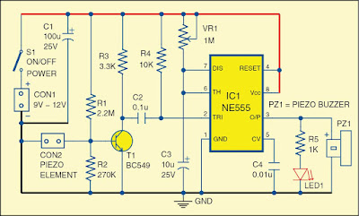
Fig. 1: Circuit of the glass break alarm

Circuit and working
  
Fig. 1 shows the circuit diagram of the glass break alarm. It is built around a piezo element connected across connector CON2, transistor BC549 (T1), timer NE555 (IC1), a piezo buzzer (PZ1) and a few other components.
A small piezo element used in the piezo buzzer is used as a sensor. It may be fixed at the centre of the window glass. IC1 is wired in monostable multivibrator mode, which is triggered by the piezo element. Output of IC1 is used to drive piezo buzzer PZ1. LED1 indicates the high-state output at pin 3 of IC1. Time delay can be adjusted by potentiometer VR1. Use an ordinary piezo buzzer at the output to generate a warning sound. This circuit works on 9V-12V DC.

When an intruder tries to break the glass, the piezo element generates an electric pulse, which is amplified and sent to the monostable multi-vibrator (IC1). The high output of IC1 drives LED1 and also produces a sound to indicate that someone is breaking the glass.

The 9V-12V DC power supply is connected across CON1, and the piezo element is connected across connector CON2.

Construction and testing
An actual-size, single-side PCB for the glass break alarm is shown in Fig. 2 and its component layout in Fig. 3. Enclose the PCB in a suitable small box in such a way that the piezo buzzer sounds when someone tries to break the glass window. Fix the piezo element at the centre of the window glass for best results.

Fig. 2: Actual-size PCB of the glass break alarm

Fig. 3: Component layout of the PCB


Use of 8-pin IC base is recommended for IC NE555.
Read More
WEARIFY

Simple Over Voltage Protector Circuit Diagram

This is the Simple Over Voltage Protector Circuit Diagram. The whole circuit of over voltage protector is build and fabricated around operational amplifier used as comparator. The inverting input is given to pin 2 of op-amp IC (IC1) with reference voltage of 5.1V from zener diode. Similarly, non-inverting input is given to pin no 3 of IC1 use as sensor for over voltage protector for sensing voltage fluctuation in the mains. The two transistors T1 and T2 conduct alternating (i.e. one at a time) according to the voltage of mains.

Simple Over Voltage Protector Circuit Diagram

Simple Over Voltage Protector Circuit Diagram


When voltage is around or below 240V AC transistor T1 is in off-state where T2 energized relay RL1. Similarly, when voltage becomes beyond 240V (i.e. above 240V) T1 is in conducting-stage and T2 is in off-stage which de-energized the relay RL1 and switch-off the appliance.

PARTS LIST

Resistors (all ¼-watt, ~+mn~ 5% Carbon)

R1 = 147 Ω/2W

R2 = 100 Ω/1W

R3 = 330 Ω

R4 = 100 KΩ

R5 = 1.8 KΩ

R6, R7 = 1 KΩ

VR1 = 10 KΩ

VR2 = 22 KΩ
Capacitors

C1, C4, C5 = 0.01 µF

C2 = 1000 µF/25V

C3 = 100 µF/25V
Semiconductors

IC1 = µA741 (Operational Amplifier)

IC2 = 7812

T1= BC547

T2 = SL100

D1, D2, D3, D4, D5 = 1N4007

D6 = 1N4148

ZD1 = 5.1V zener diode
Miscellaneous

X1 = 230V AC primary to 7.5V-0-7.5V, 1A secondary transformer

RL1 = 12V, 200Ω 1 C/O Relay

LED1 = RED
Read More
WEARIFY

A Handy Pen Torch Circuit Diagram

This easy to construct “Handy pen torch” electronic circuit and low component count, uses two power white LEDs for lighting. Low volt (4.8V dc) supply available from the built in rechargeable Ni-Cd battery pack is first converted into two channel (independent) constant current sources by two pieces of the renowned precision adjustable shunt regulator chip LM334 (IC1 and IC2). Around 25mA at 3.6 volt dc is available at the output of these ICs.

This regulated dc supply is used to drive two power white LEDs D4 and D6. Resistors R3 and R5 limits the output current (and hence the light output) of IC1 and IC2 circuits respectively. Besides these components, one red color LED (D2) is included in the main circuit which works as a battery charging supply input indicator. Resistor R1 limits the operating current of this LED.

Pen Torch Electronic Circuit Schematic

A Handy Pen Torch Circuit Diagram


Diode D1 works as an input polarity guard cum reverse current flow preventer. Capacitor C1 is a simple buffer for circuit stabilization. After succesful construction, preferably on a small piece of general purpose PCB, enclose the whole circuit in a suitable and attractive pen torch cabinet. If necessary, drill suitable holes in the cabinet to attatch the dc socket, on/off switch and the input indicator etc. In prototype,commonly available 4.8 volt/500mah Ni-Cd battery pack (for cordless telephones) is used.

One very simple but reliable ac mains powered battery charger circuit for the handy pen torch is also included here. Basically the pen torch circuit is a constant current charger wired around Transistor T1 (BC636), powered by a 12v/350mA step down transformer and associated componentsD1, D2 and C1.

AC mains powered battery charger for the pen torch


A Handy Pen Torch Circuit Diagram
Unregulated 12 volt dc available from the input power convereter circuit, comprising step down transformer(TRF), rectifier diodes (D1,D2) and filter capacitor (C1), is fed to T1 through a current limiting resistor R1. Grounded base PNP transistor T1 here works as a constant current generator. With 22 ohm resistor for R1, the charging current available at the output of the charger is near 50mA.

Red LED (D3) provides a fixed voltage reference to the base of T1, with the help of resistor R2. (During charging process, Diode D1 in the main circuit prevent reverse current flow from the battery pack when charging input supply is absent.) After construction of the pen torch circuit, fit the assembled unit inside a small plastic enclosure for safety and convenience.
Read More
WEARIFY

Electronic siren circuit Diagram

This is a compact electronic siren circuit based on three transistors.This circuit is suitable for in corporating with other alarm or siren projects such as burglar alarms, automatic factory sirens etc or a simple push to on alarm.

The  electronic siren circuit given here  is  based on a complementary transistor pair consisting of Q2 & Q3 (BC557 & BC 37)  wired as an astable multivibrator oscillator,which directly drives the speaker.The transistor Q1 is used to provide a full charge on capacitor C2 when power is turned ON. When push button switch S1 is pressed , the capacitor C2 slowly discharges through resistor R8.This makes the circuit to  oscillate at a low frequency that increases to a high frequency and kept indefinitely as the capacitor is fully discharged. When the switch P1 is released, the output  frequency decreases slowly as C2 is charged to the  positive voltage through resistance R6 and the Base-Emitter junction of tramsistor Q2. When C2 is fully charged to the positive battery voltage the  circuit stops oscillating.

Electronic siren circuit Diagram with Parts list.

Electronic siren circuit Diagram


Notes.


  • A 12 V battery or a a well regulated 12V DC power supply can be used to power the circuit.
  • Assemble the circuit on a good quality PCB or common board.
  • The switch S1 can be used to activate the alarm.
  • The switch S2 can be used as a power switch.
  • You can experiment on the tone of alarm by using different values for C2 and R8.
Read More
WEARIFY

Simple 3-in-1 Flash Light Project

Want to avoid the problem of carrying three different flashlights to perform a test? Why don’t you try integrating Ultra Violet, Infra Red and visible light together in one flashlight? Read on to know more about this.

The multi-tasking flashlight is basically composed of a metallic case, a switch, cables and connections, four 9V batteries and three different LED heads that provide the desired light beam. For the construction of this flashlight, LedEngin’s LZ4-40 is recommended. This comes with a very wide wavelength that includes infra red and ultra violet light. Distinct visible light color temperature can also be found.
Flash Light Project


Flash Light Project

The first step is to build the body of the flashlight, using an aluminum tube. Next come the drilling and cutting for switches and covers. Once the body is finished, the work on the constant current driver should be completed, adding the proper terminals for the batteries and the base for the LED heads.

Once all the power source wiring is completed and insulated with heat shrink tubing, the LED heads are assembled and connected. These are basically composed of an aluminum cap. The LED base and the power source connections come from the batteries.
Read More
WEARIFY

Automotive Turn Flasher with lamp output Detection

Here is a circuit of a flasher which I designed for automotive use. It has a built-in function of lamp-outage detection. In normal operation, it will flash at about 1.4Hz and when a lamp goes bad, the flash-rate is doubled. The flashers faster clicking sound and the dashboard indicators faster flashing attracts the drivers attention that one of the bulbs has gone out.

Automotive Turn Flasher with lamp  output Detection:


Automotive Turn Flasher with lamp output Detection


Notes
The circuit consists of two parts - the flashing unit and the lamp outage detection module. The flashing unit is built around 555 timer configured as an astable multivibrator. The resistors R12/R13 and capacitors C3/C4 sets the required frequency. Note that C3 is connected in parallel to C4 through BC547 an NPN transistor, acting as a switch. When there is positive voltage at the base of the transistor, it conducts and connects C3 to ground. C3 & C4 in parallel doubles the capacitance value i.e. 220nF + 220nF = 440nF. This capacitance value together with R12 and R13 result in frequency of about 1.4Hz.

In the lamp outage detection module, a shunt resistor (a thick wire) with a calculated minor resistance (30mΩ) is the key to detect the lamp outage. The voltage to lamps is fed thru this shunt. Hence, the shunt is connected in series to the network of the bulbs which are connected in parallel. The inverting input of the comparator U1 is also connected to the shunt. The non-inverting input is connected to a potential divider providing a reference voltage of 11.90V

NORMAL OPERATION:

Square wave between 11.89V - 12.0V at (-)ve input of U1
11.90V (reference voltage) at (+)ve input of U1

The comparator U1 compares these voltages and the output is a square wave between 0-12V. This output is rectified through diode D1 and filtered through capacitor C1. Now, we have a triangular wave form which is fed into another comparator U2.

1V (reference voltage) at the (-)ve input of U2 and
a triangular wave between 7V - 8V at (+)ve input of U2
OPERATION WITH A DEFECTIVE LAMP: OPERATION WITH A DEFECTIVE LAMP:
When a bulb is defective, there is an increase in the resistance of the bulb network hence the voltage drop across the shunt is changed. So, in this case we would have:

Square wave between 11.95V - 12.0V at (-)ve input of U1
11.90V (reference voltage) at (+)ve input of U1

The comparator U1 compares them and the output is almost zero volts. After the diode and the filter network, we finally have a few millivolts at the +input of U2 which is compared with the reference voltage, 1V. This results in low output of U2 which ultimately switches off the NPN and hence C3 is disconnected from the ground.

Now, the timing network of 555 has only C4 to work with, therefore the frequency of the oscillation is doubled. This causes the remaining bulbs to flash at doubled rate.

NOTE:
A single quad op-amp IC LM324 could also be used for building this circuit. Two of the op-amps to be used as comparators in place of U1 & U2. Another op-amp can be configured as astable oscillator in place of 555 to flash the bulbs. This astable oscillator will have two timing capacitors as used above with 555.
Read More
WEARIFY

Simple Fog Lamp Sensor

For several years now, a rear fog lamp has been mandatory for trailers and caravans in order to improve visibility under foggy conditions. When this fog lamp is switched on, the fog lamp of the pulling vehicle must be switched of to avoid irritating reflections. For this purpose, a mechanical switch is now built into the 13-way female connector in order to switch of the fog lamp of the pulling vehicle and switch on the fog lamp of the trailer or caravan. For anyone who uses a 7-way connector, this switching can also be implemented electronically with the aid of the circuit illustrated here.

Fog Lamp Sensor Circuit Diagram:

Simple Fog Lamp Sensor

Here a type P521 optocoupler detects whether the fog lamp of the caravan or trailer is connected. If the fog lamp is switched on in the car, a current flows through the caravan fog lamp via diodes D1 and D2. This causes the LED in the optocoupler to light up, with the result that the photo-transistor conducts and energies the relay via transistor T1. The relay switches of the fog lamp of the car. For anyone who’s not all thumbs, this small circuit can easily be built on a small piece of perforated circuit board and then fitted somewhere close to the rear lamp fitting of the pulling vehicle. Link
Read More
WEARIFY

Automatic fan controller


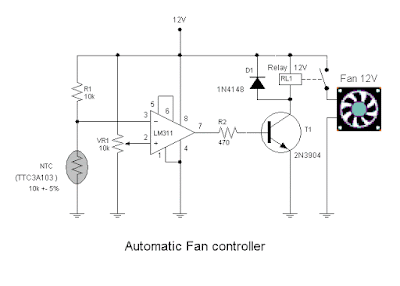
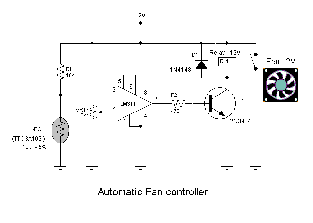
This circuit will turn on/off 12V DC fan or CPU fan when temperature above normal temperature.You can set turn on temperature by adjust VR1.

Automatic fan controller Circuit Diagram:


Automatic fan controller


This circuit use an NTC (Negative temperature coefficient)which is a thermistor is one in which the zero-power resistance decreases with an increase in temperature. So If temperature increate the voltage at pin 3 on LM311 will decreated .The resistance of NTC is about 10K at 25'c.

VR1 should be multi-turn potentiometer type such 10K/25 turn.
Sourced By : W3 Circuits
Read More
WEARIFY

Temperature Candle Using LED

LED based projects require a lot of skill and hence only experienced circuit designers try out these circuits. But there are also a few circuits in this genre that can be done by amateur electronic hobbyists. The temperature candle is one such circuit. Read on to know more about this.

Temperature Candle Using LED

The hardware components that are required to build this circuit are listed below:


  • Microcontroller
  • Temperature Sensor
  • RGB LED
  • PCB


The circuit design is pretty simple. The LED is made to flicker by the microcontroller and the color is based on the ambient temperature at that point. The temperature of the room can be known by observing the color of the LED.

The temperature value is obtained in degree Celsius. This value is received as a result of pressing the reset button on the PCB. This value can also be obtained by providing power to the device. Once the device is powered up, the change in temperature is indicated. The blue LED is triggered for a temperature increase of 10 degrees. The red LED is triggered for a temperature increase of a single degree.

Suppose, the ambient temperature is 23 degrees celsius, The circuit works in such a way that the blue LED is made to blink twice and the red LED is made to blink 3 times. Soon after this, an orange colored flicker is observed as the LED goes into canfle mode.

Since through hole components are used in this circuit, it is very cheap to construct and the components can be easily soldered. The circuit also contains a jack for connecting to a Microchip Pickit 3 programmer / debugger. This reduces the complexity involved in code modification and download.

Sourced By : W3 Circuits
Read More