Showing posts with label Amplifier. Show all posts
WEARIFY

MT8870 DTMF Telephone Dial Tone Decoder Circuit Diagram

Build a MT8870 DTMF Telephone Dial Tone Decoder Circuit Diagram. This is a  simple MT8870 DTMF Telephone Dial Tone Decoder Circuit Diagram. In this circuit one common DTMF receiver IC is the Motorola MT8870 that is widely used in electronic communications circuits. The MT8870 isan 18-pin IC. It is used in telephones and a variety of other applications. When a proper output is not obtained in projects using this IC, engineers or technicians need to test this IC separately. 

A quick testing of this IC could save a lot of time in research labs and manufacturing industries of communication instruments. Here’s a small and handy tester circuit for the DTMF IC. It can be assembled on a multipurpose PCB with an 18-pin IC base. One can also test the IC on a simple breadboard. For optimum working of telephone equipment, the DTMF receiver must be designed to recognize a valid tone pair greater than 40 ms in duration and to accept successive digit tone-pairs that are greater than 40 ms apart. 

 MT8870 DTMF Telephone Dial Tone Decoder Circuit Diagram

MT8870 DTMF Telephone Dial Tone Decoder Circuit Diagram

Read More
WEARIFY

Telephone for VoIP gate Circuit Diagram

A project of Telephone for VoIP gate Circuit Diagram. Calls over the Internet can be in several different ways. For households with a permanent connection to the Internet, it is advantageous to use different IP phones and VoIP gateways that need to function on the computer. Because IP phones are still relatively expensive, they are used more often different VoIP gateway. VoIPgateway is "one end" connected to a network with access to the internet, the "other end" connects a standard analog phone, which is then used in the normal way and that has given a telephone number available from any fixed or mobile phone. Some VoIP gateway router in addition to that we need as well, if we want to access via a modem to connect multiple computers. To my VoIP gateway, we can connect nehomologovaný, self made ​​phone. Instructions for simple phone is the subject of this article.

How to the phone works

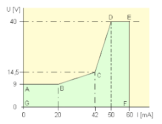
Normally the phone line is a DC voltage, usually 50 to 70 V. During the ringtone to this voltage superposed yet AC 50-100 V with a frequency of usually 20 or 25 Hz. "Pick up the 'phone line will pass through the current 20-40 mA. On the phone while the voltage drop occurs several volts (Fig. 1). This voltage can be used to power the circuitry phone. The polarity of the DC voltage is not defined, the phone must function in both polarities. The phone line is when answering the call of a defined impedance, which should be adapted telephone. Line impedance in different countries vary so as the phone purchased in Germany (impedance 220 ​​ohms + 820 ohms in parallel with 220 nF) not in Bohemia (600 ohms) to work optimally. Sometimes differ impedance different networks within the same country, depending on the age and type of telephone exchanges, length and characteristics of the cables.

Fig. 1 The voltage on the raised phone

Fig. 1 The voltage on the raised phone would, depending on the passing stream should be in the area indicated by the letters A to G

The most important part of the phone is a colloquial circuit. The call is transmitted over the line modulation current that flows through the line. The current is modulated on the side panel (VoIPGateway), which transfers the call to the user, and in the device, which is transmitted from the user. The speech circuit is a hybrid circuit that suppresses the signal from the microphone in the earpiece. The hybrid circuit is on the opposite side (PBX, VoIP gateway). The hybrid circuit is usually some sort of bridge, and therefore it is necessary to impedance phone and VoIP gateway (or exchange) have been adapted. It is important especially for VoIP devices, where the influence of digitization and transmission of data over the Internet arises signal delay in the order of tens of milliseconds. Mismatch, especially on the VoIP gateway, there is a very annoying echo.

Fig 2nd Simple telephone hybrid circuit

Fig. 2 Colloquial hybrid transformer circuit. If L1 and L2 have the same number of threads and balancing impedance ZM is equal to the line impedance ZL, the microphone signal in the handset suppressed


Another important part of the circuit for dialing. All modern devices support tone dialing. Ringing circuit to alert the user to an incoming call. Acoustic (bell) or optical signals indicates the presence of ringing voltage on the line. Hook switch is a switch that turns on the circuit colloquial answer the phone.

Specifications


Telephone impedance:
aprox. 600 Ohm.

Recomended line impedance:
real. 600 Ohm.

Operating (off-hook) current:
20 mA
(10 to 40 mA.)

Operating voltage:
aprox. 7 V @ 20 mA.
 Dialing:DTMF

"In-use" indication:
3 to 15 V/ aprox. 1 mA

On-hook current:
aprox. 0,01 mA @ 50 V


Phone Circuit Schematic

Fig 3rd Telephone unit schematic


Fig 3rd Telephone unit schematic

Connection phone in Figure 3 Colloquial circuit with transistors T1 to T3 is connected via a hook switch and bridge DB1 to the telephone line . Diode bridge ensures that electronic circuits are supplied with the correct polarity. If the hook switch is closed, current passes through the transistor T1 lines , which is used as microphone amplifier and transistors T2 and T3 , which amplifies the signal to the receiver. Headphone amplifier operates in class A. The amplitude of the output voltage at the collector of the transistor is about 1 V, which for the purpose of completely sufficient . Headphones or speakers can be used with an impedance of 8 ohms , the amplifier but works better (has lower distortion) with higher impedance load . Trimmer P2 can adjust the gain as needed.

The amplifier is continuously drop of about 1.3 V, the sum of the voltage UBE transistors T2 and T3 and is only slightly dependent on the flowing current. This voltage across the resistor R1 is powered electret microphone . The signal from the microphone passes through C1 to the base of transistor T1 . It amplifies the signal level required to excite the line. Originally, the microphone amplifier much more difficult . But he had unnecessarily high gain and output impedance inappropriate . This simple connection works better . Working point T1 is set resistors R2 to R4 . The microphone amplifier there is a voltage drop of about 3.5 V , the voltage drop can be under current amplification T1 changed 3 to 4 V. Resistor R5 introduced at this stage, a negative feedback regulating the amplification and decreasing distortion. Balancing circuit C6, R6 and P1 suppresses the signal from the microphone in headphone amplifier .

The signal from the microphone is on the collector of T1 opposite phase than the emitter , but the amplitude of the signal at the collector is much greater. Potentiometer P1 can set a condition where the signals from the collector and emitter of the capacitor C7 T1 readings and audio from the microphone in the handset is suppressed. Simplified diagram balancing the bridge is in Figure 4 The setting is very dependent on the impedance of the line. Because VoIP gateway creates a link with the active resistance of 600 ohm and short supply does not create a significant reactive component , the setting is simple and very effective. The signal coming from the gateway or PBX is the collector and emitter of T1 phase balancing circuit and is therefore not suppressed.

Fig. 4th Simplified wiring hybrid (balancing) circuit in the phone

Fig. 4th Simplified wiring hybrid (balancing) circuit in the phone

In order to suppress its signal worked well on the VoIP gateway, you need the phone to be defined impedance close to the impedance of the gate, ie 600 ohm. The output impedance of the collector T1 for AC signals, large, almost current source. Impedance of the phone for voice signals are essentially a parallel combination of R6, R1 and about one order larger impedance collector T1. Rectifier bridge through which the signal passes, it will affect the impedance to a minimum.

 Fig 5 Dialer circuit arrangement
 Fig 5 Dialer circuit arrangement

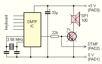
For DTMF I did not find any suitable integrated circuit , and generate DTMF signal discrete oscillators would be difficult and impractical . Finally, I modified the DTMF phone dialer . Dialer is a small box with buttons and speaker , generating tones when you press the button corresponding to the relevant figures. It is used for remote telephone answering and for the selective choice of the civil radio stations . The dialer (Fig. 5 ), the signal goes from the integrated circuit via the 22k resistor on the transistor, which drives a small speaker . Transistor speaker and I vymontoval a DTMF signal is connected to the transistor T4 on the phone. After pressing the button, the IO output voltage appears about 1 V with superimposed DTMF signal . Connect the telephone line is very simple, just enough transistor T4 and resistor R7. The change in resistance R7 can adjust the intensity of tone . Speaker of the phone dialer I used it as a handset . Dialer , according to the type of memory to 11 or 13 numbers , but unfortunately it lacks useful the " Redial" to repeat the last number called. I could not deal with power dialer from the phone line , so your phone is a small battery , which is likely to last for many years. The battery has an advantage in that it forgets the stored phone numbers if you disconnect it from the line.

Also, the ringing circuit I did not get special IO . That's why I like bell oscillator is used samovybuzujícím a piezoelectric transducer . The oscillator is fed stream that passes through the ringer capacitor C8 , bridges DB2 , LED2 to LED4 and resistor R14 . The oscillator is operated only in one half , the sound is more significant . In the other half cycle current through diode D1 . The bell must have a dead zone . That there is provided connecting the LED. Ringing voltage amplitude must have at least 10 V to Buzzer began publishing a sound. The phone I used a blue LED with high luminance. These intensely lit even at current several milliamps , which is ringing flow. LED also serves as a visual alarm bell , which could be useful in noisy environments .

The last telephone circuits are busy lamp . Phone I was seeking a second phone in parallel connected to the device at the other end of the apartment . When the phone is " suspended " , the hook switch is switched to the circuit with transistors T5 and T7 . If all telephones on the line hung on the line voltage of 50 to 60 V. The transistor T5 is opened, closed, and T7 LED1 off. The circuit is taken from the line is very little current through resistors R8 and R9 . Shrinks if the line voltage is below 15 V, T5 is closed , opens T7 and LED1 lights up. Transistor T6 T7 gate bias control by the loss of the R11 so that LED1 is energized about 1 mA , which is quite sufficient for display . In the voltage range of 3-15 V line lights LED1 virtually the same. BSS123 transistor has a maximum voltage UDS only 100 V. If the ringtone is this voltage is exceeded. In my phone's built higher voltage transistor has lasted several months . If you're worried about him , you can type BS108 with UDSmax 200 V, but it is not in SMD . The "in use" circuit not be planted, if you indicate you do not need , or can be used alone for another phone .

Mechanical Design

Width of the printed circuit board was designed dimensions dialer , then the length of a "reasonable " distance between the microphone and earpiece. Although the board is a lot of space , most of SMD components . They take up less space and is easier mounting plate is not so much tinkering . Figure motive circuit and layout of components , following table .


Mechanical Design

Before you assemble components, prepare the first dialer and attach it to desce.Z dialer remove the battery and remove the hinged cover. Dialer carefully "crack". It should go fairly easily if you start in the corner, to which is attached a chain. Odpájíme the speaker wires from the board dialer and speaker carefully shucks from the bottom of the box. The board dialer vypájíme more transistor in TO92. The board dialer solder short wires to negative (Pad1) and positive (PAD3) terminal electrolytic capacitor and terminal for transistor-based vypájeného (PAD2). Editing is perhaps evident from Figure 9 photos The lower part of the housing dialer yet only tentatively secured to the plate phone plastic rivets (Fig. 10). We remove the box and the board will be filled by phone components.

 Fig. 6th Editing dialer and connection terminals
 Fig. 6th Editing dialer and connection terminals


Phone was originally in a transparent plastic box, which was inside the LED backlight. Its production, however, I not successful, so I made ​​a wooden box. To her I used plywood manufacture of soft wood, obtained from the fruit of hazel. That will free devoted almost everyone greengrocer. From one high hazels get material for a few boxes. Plywood is easily machined and well bonded dispersion adhesive. I eventually recut the box, namoÅ™il and pÅ™elakoval polyurethane varnish.

 Fig. 7th Mounting boxes dialer
 Fig. 7th Mounting boxes dialer

With the change in boxes I had to adjust some components on the board. LEDs were originally all SMD. Finally, there were only SMD LED 2. But it is not visible from the outside, and therefore does not need much light. You can replace the zener diode (3-12 V) or short-circuit, but it increases the sensitivity of the ringing circuit. Other LED in case of 3 mm diameter. It turns out that it is better to use LED with high luminous than type 2 mA of current, because the small stream shines more. Also switch SW1 on the phone "lifting", I moved to the side boards. Deferred phone is on the table laid down the keyboard. LED on the back because they are easy to see and switch is when you pick up the phone available with one touch. Of the joints it can not be soldered to the board just because they do not get tipped soldering iron to solder pad. On the solder contacts because I rozklepl small rivets, which I soldered joints by.

I then links to the rivets inserted the switch and soldered it from the opposite side of the board. Between the switch and the plate I put a piece of insulating paper. The switch can also be placed at any other suitable location in the box and board interconnect wires. Switches P-B143 of the newer series ("silver") are not too good and We turn the lever sometimes lose contact. To fix it so that "packs" pertinax holding plate with pins a little more same hopper. The defect had all the pieces that I had at home. Dimensionally the same switch, but painted black were fine.

Fig. 8th The top side of the printed circuit board
 Fig. 8th The top side of the printed circuit board


The power dialer instead of the original articles I used lithium batteries. Do you solder boards phone as housing purchased as the GM and housing that vypájíte of defective motherboards PC that has otherwise placed pins. Piezoelectric transducer is bolted small screws through the PCB to the bottom of the box dialer.
On the microphone I slid the piece of tubing so that the tubing fit snugly inside the box. Thus reducing the acoustic coupling between the earpiece and microphone inside the device.

Fig. 9th The underside of the plate and box
 Fig. 9th The underside of the plate and box


Fig. 10th The back of the phone with LED switch and a hole for the bell

Fig. 10th The back of the phone with LED switch and a hole for the bell

Animation

Phone use in conjunction with the gateway Linksys Sipura SP2100. In the firewall settings to make sure that in menu / admin / voice / advanced tab you have set up Regional impedance lines FXS Port Impedance: 600 Phone can revive a product as shown in Figure 14 (SW1 closed). You can test with a different phone when line current, measure the voltage on the line and estimate the impedance of the phone - AC voltage test point should be after the switch opens twice. The trimmer P2 dial to maximum resistance (max volume). To attach the microphone sound source (eg mp3 player headphones) and adjust the trimmer P1 so that the sound from the microphone not hear the telephone handset. Try tone. Ringing circuit you can try connecting the phone via a suspended resistor 1 kOhm to AC voltage 24-50 V.

 Fig. 11th test preparation
 Fig. 11th test preparation

Conclusion

The phone is in operation for several months and yet it was conceived as a second auxiliary telephone is often used. I have tested it successfully on the public switched telephone network (PSTN), but because I'm not sure whether it meets all required standards, there should not be connected. PSTN to VoIP gateway over a larger voltage when hanging up a more current when the phone is picked up.

List of components
 
R14,7 kOhm, SMD 1206
R21 kOhm, SMD 1206
R3, R422 kOhm, SMD 1206
R533 Ohm, SMD 1206
R62,2 kOhm, SMD 1206
R7220 Ohm, SMD 1206
R8, R910 MOhm, SMD 1206
R10330 kOhm, SMD 1206
R11470 Ohm, SMD 1206
R12220 kOhm, SMD 1206
R13, R1410 kOhm, SMD 1206
P1250 Ohm, trimr PT6V (Piher)
P25 kOhm, trimr PT6V (Piher)
C1220 nF, SMD 1206
C210 mikroF/16 V, tantalum., SMD B
C31000 mikroF/6,3 V, electrolytic
C4, C5100 mikroF/6,3 V, tantalum, SMD D
C647 mikroF/16 V, tantalum., SMD D
C74,7 mikroF/10 V, tantalum, SMD A
C8220 nF/250 V, foil MKT RM5
PCB board bcs59

D11N4148SMD, SOD80
DB1, DB2S250,mini DIP bridge
ZD1BZV55C15SMD, Zener. diode 15 V SOD80
T1, T3BC817-40, SOT-23
T2BC807-40, SOT-23
T4 až T6, T8BC848C, SOT-23
T7BSS123, SOT-23 (BS108, TO92)
LED1high intensity 3 mm red LED (it's better than 2 mA LED)
LED2any 3 mm SMD LED or Zener diode 3 to 12 V
LED3, LED4high intensity 3 mm blue LED (it's better than 2 mA LED)
MIC1elektret. mikrofon MCE100
SP1tiny speaker or headphone 100 Ohm (8 to 100 Ohm),
removed from dialer
B1CR2032 battery and holder
SW1 P-B143, SPST switch
K1slim RJ11 plug WEBP 6-4 LP
SP2piezo KPT2038FW
dialerdialer DTMF 13 or 11
Read More
WEARIFY

Telephone Record Control Circuit Diagram

This circuit will allow you to connect any tape recorder that has a mic and remote input to a phone line and automatically record both sides of a conversation when ever the phone is in use. You will need to take a couple of voltage readings before connecting the circuit. First determine the polarity of your phone line and connect it to the circuit as shown and then determine the polarity of the remote input and connect it to the circuit. Circuit operation is as follows. When the phone is on hook the voltage across the phone line is about 48volts dc. When the phone is off hook the voltage will drop to below 10volts dc. When the line voltage is at 48volts the FET is off which causes Q2 and Q3 to be off. When the phone is picked up the FET turns on along with Q2 and Q3 which turns your recorder on. The tape recorder must be in the record mode at all times. As you can see the power source for the circuit is the phone line.

Circuit Diagram


Telephone Record Control Circuit Diagram

Read More
WEARIFY

Automatic Headlight Brightness Switch Project

Driving the highway with your high-beam headlights can really increase your visibility, but can be a blinding hazard for other drivers. This simple circuit can be wired into your headlight switch to provide automatic switching between high and low beam headlights when there is oncoming traffic. It does this by sensing the lights of that traffic. In this way, you can drive safely with your high-beams on without blinding other drivers.

Automatic Headlight Brightness Switch Circuit Diagram

Automatic Headlight Brightness Switch Project


Parts

Part    Total Qty    Description
R1              1         5K 1/4W Resistor   
R2,R3,R4   3         5K Pot   
Q1              1         NPN Phototransistor   
Q2              1         2N3906 PNP Transistor   
K1              1         Low Current 12V SPST Relay   
K2              1         High Current 12V SPDT Relay   
S1               1         SPST Switch   
B1               1         Car Battery   
MISC          1         Case, wire, board, knobs for pots   

Notes

Q1 should me mounted in such a way so it points toward the front of the car with a clear line of site. Suitable places are on the dashboard, in the front grill, etc.
Adjust all the pots for proper response by testing on a deserted road.
S1 enables and disables the circuit.
B1 is, obviously, in the car already.
Before you try to connect this circuit, get a wiring diagram for your car. Some auto manufacturers do weird things with wiring.
Connection A goes to the high beam circuit, B goes to the headlight switch common and C connects to the low beam circuit.
Read More
WEARIFY

Glass Break Alarm Circuit Diagram

This circuit can be used for sounding an alarm to detect the breaking of a glass window by an intruder, even when the intruder ensures there is no sound of the shattered glass.
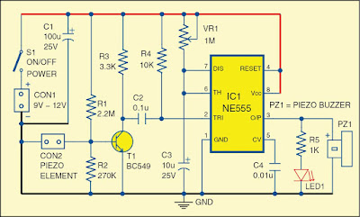
Fig. 1: Circuit of the glass break alarm

Circuit and working
  
Fig. 1 shows the circuit diagram of the glass break alarm. It is built around a piezo element connected across connector CON2, transistor BC549 (T1), timer NE555 (IC1), a piezo buzzer (PZ1) and a few other components.
A small piezo element used in the piezo buzzer is used as a sensor. It may be fixed at the centre of the window glass. IC1 is wired in monostable multivibrator mode, which is triggered by the piezo element. Output of IC1 is used to drive piezo buzzer PZ1. LED1 indicates the high-state output at pin 3 of IC1. Time delay can be adjusted by potentiometer VR1. Use an ordinary piezo buzzer at the output to generate a warning sound. This circuit works on 9V-12V DC.

When an intruder tries to break the glass, the piezo element generates an electric pulse, which is amplified and sent to the monostable multi-vibrator (IC1). The high output of IC1 drives LED1 and also produces a sound to indicate that someone is breaking the glass.

The 9V-12V DC power supply is connected across CON1, and the piezo element is connected across connector CON2.

Construction and testing
An actual-size, single-side PCB for the glass break alarm is shown in Fig. 2 and its component layout in Fig. 3. Enclose the PCB in a suitable small box in such a way that the piezo buzzer sounds when someone tries to break the glass window. Fix the piezo element at the centre of the window glass for best results.

Fig. 2: Actual-size PCB of the glass break alarm

Fig. 3: Component layout of the PCB


Use of 8-pin IC base is recommended for IC NE555.
Read More
WEARIFY

Simple Over Voltage Protector Circuit Diagram

This is the Simple Over Voltage Protector Circuit Diagram. The whole circuit of over voltage protector is build and fabricated around operational amplifier used as comparator. The inverting input is given to pin 2 of op-amp IC (IC1) with reference voltage of 5.1V from zener diode. Similarly, non-inverting input is given to pin no 3 of IC1 use as sensor for over voltage protector for sensing voltage fluctuation in the mains. The two transistors T1 and T2 conduct alternating (i.e. one at a time) according to the voltage of mains.

Simple Over Voltage Protector Circuit Diagram

Simple Over Voltage Protector Circuit Diagram


When voltage is around or below 240V AC transistor T1 is in off-state where T2 energized relay RL1. Similarly, when voltage becomes beyond 240V (i.e. above 240V) T1 is in conducting-stage and T2 is in off-stage which de-energized the relay RL1 and switch-off the appliance.

PARTS LIST

Resistors (all ¼-watt, ~+mn~ 5% Carbon)

R1 = 147 Ω/2W

R2 = 100 Ω/1W

R3 = 330 Ω

R4 = 100 KΩ

R5 = 1.8 KΩ

R6, R7 = 1 KΩ

VR1 = 10 KΩ

VR2 = 22 KΩ
Capacitors

C1, C4, C5 = 0.01 µF

C2 = 1000 µF/25V

C3 = 100 µF/25V
Semiconductors

IC1 = µA741 (Operational Amplifier)

IC2 = 7812

T1= BC547

T2 = SL100

D1, D2, D3, D4, D5 = 1N4007

D6 = 1N4148

ZD1 = 5.1V zener diode
Miscellaneous

X1 = 230V AC primary to 7.5V-0-7.5V, 1A secondary transformer

RL1 = 12V, 200Ω 1 C/O Relay

LED1 = RED
Read More
WEARIFY

Electronic siren circuit Diagram

This is a compact electronic siren circuit based on three transistors.This circuit is suitable for in corporating with other alarm or siren projects such as burglar alarms, automatic factory sirens etc or a simple push to on alarm.

The  electronic siren circuit given here  is  based on a complementary transistor pair consisting of Q2 & Q3 (BC557 & BC 37)  wired as an astable multivibrator oscillator,which directly drives the speaker.The transistor Q1 is used to provide a full charge on capacitor C2 when power is turned ON. When push button switch S1 is pressed , the capacitor C2 slowly discharges through resistor R8.This makes the circuit to  oscillate at a low frequency that increases to a high frequency and kept indefinitely as the capacitor is fully discharged. When the switch P1 is released, the output  frequency decreases slowly as C2 is charged to the  positive voltage through resistance R6 and the Base-Emitter junction of tramsistor Q2. When C2 is fully charged to the positive battery voltage the  circuit stops oscillating.

Electronic siren circuit Diagram with Parts list.

Electronic siren circuit Diagram


Notes.


  • A 12 V battery or a a well regulated 12V DC power supply can be used to power the circuit.
  • Assemble the circuit on a good quality PCB or common board.
  • The switch S1 can be used to activate the alarm.
  • The switch S2 can be used as a power switch.
  • You can experiment on the tone of alarm by using different values for C2 and R8.
Read More
WEARIFY

300 Watt Subwoofer Power Amplifier Circuit Diagram

The output devices are MJL4281A (NPN) and MJL4302A (PNP), and feature high bandwidth, excellent SOA (safe operating area), high linearity and high gain. Driver transistors are MJE15034 (NPN) and MJE15035 (PNP). All devices are rated at 350V, with the power transistors having a 230W dissipation and the drivers are 50W.

Having built a P68 using these transistors, I recommend them highly - the amplifier is most certainly at its very best with the high gain and linearity afforded by these devices. Note that there are a few minor changes to the circuit (shown below).

High power amps are not too common as projects, since they are by their nature normally difficult to build, and are expensive. A small error during assembly means that you start again - this can get very costly. I recommend that you use the PCB for this amplifier, as it will save you much grief. This is not an amp for beginners working with Veroboard!

The amplifier can be assembled by a reasonably experienced hobbyist in about three hours. The metalwork will take somewhat longer, and this is especially true for the high continuous power variant. Even so, it is simple to build, compact, relatively inexpensive, and provides a level of performance that will satisfy most requirements.

300W Sub woofer Power Amplifier Circuit Diagram

Build a 300 Watt Subwoofer Power Amplifier Circuit Diagram

Fig 1
WARNINGS:
  • This amplifier is not trivial, despite its small size and apparent simplicity. The total DC is over 110V, and can kill you.
  • The power dissipated is such that great care is needed with transistor mounting.
  • The S300 is intended for intermittent duty on 4 Ohm loads, as will normally be found in a subwoofer. It is NOT intended for PA or any other continuous duty, and although it may work fine for may years, I absolutely do not recommend this.
  • For continuous duty, do not use less than 8 Ohms.
  • There is NO SHORT CIRCUIT PROTECTION. The amp is designed to be used within a subwoofer enclosure, so this has not been included. A short on the output will almost certainly destroy the amplifier.
DO NOT ATTEMPT THIS AMPLIFIER AS YOUR FIRST PROJECT

Please note that this amp is NOT designed for continuous high power into 4 Ohms. It is designed for intermittent duty, suitable for an equalized sub woofer system (for example using the ELF principle - see the Project Page for the info on this circuit). Where continuous high power is required, another 4 output transistors are needed, wired in the same way as Q9, Q10, Q11 and Q12, and using 0.1 ohm emitter resistors.

Continuous power into 8 ohms is typically over 150W, and it can be used in the form shown at full power into an 8 ohm load all day, every day. The additional transistors are only needed if you want to do the same thing into 4 ohms!

The circuit is shown in Figure 1, and it is a reasonably conventional design. Connections are provided for the Internal SIM (published elsewhere on the Project Pages), and filtering is provided for RF protection (R1, C2). The input is via a 4.7uF bipolar cap, as this provides lots of capacitance in a small size. Because of the impedance, little or no degradation of sound will be apparent. A polyester cap may be used if you prefer - 1uF with the nominal 22k input impedance will give a -3dB frequency of 7.2Hz, which is quite low enough for any sub.
The input stage is a conventional long-tailed pair, and uses a current sink (Q1) in the emitter circuit. I elected to use a current sink here to ensure that the amp would stabilise quickly upon application (and removal) of power, to eliminate the dreaded turn on "thump". The amp is actually at reasonably stable operating conditions with as little as +/-5 volts! Note also that there are connections for the SIM (Sound Impairment Monitor), which will indicate clipping better than any conventional clipping indicator circuit. See the Project Pages for details on making a SIM circuit. 
The Class-A driver is again conventional, and uses a Miller stabilisation cap. This component should be either a 500V ceramic or a polystyrene device for best linearity. The collector load uses the bootstrap principle rather than an active current sink, as this is cheaper and very reliable (besides, I like the bootstrap principle :-)

All three driver transistors must be on a heatsink, and D2 and D3 should be in good thermal contact with the driver heatsink. Neglect to do this and the result will be thermal runaway, and the amp will fail.

C11 does not exist on this schematic, so don't bother looking for it. It was "mislaid" when the schematic was prepared, and I didn't notice until someone asked me where and what it was supposed to be. Sorry about that.
It is in the output stage that the power capability of this amp is revealed. The main output is similar to many of my other designs, but with a higher value than normal for the "emitter" resistors (R16, R17). The voltage across these resistors is then used to provide base current for the main output devices, which operate in full Class-B. In some respects, this is a "poor-man's" version of the famous Quad "current dumping" circuit, but without the refinements.

Although I have shown MJL4281A and MJL4302A output transistors, because they are new most constructors will find that these are not as easy to get as they should be. The alternatives are MJL21193/ MJL21194
Build a 300 Watt Subwoofer Power Amplifier Circuit Diagram
Fig 2

Note: It is no longer possible to recommend any Toshiba transistors, since they are the most commonly counterfeited of all. The 2SA1302 and 2SC3281 are now obsolete - if you do find them, they are almost certainly fakes, since Toshiba has not made these devices since around 1999~2000.

Use a standard green LED. Do not use high brightness or other colors, as they may have a slightly different forward voltage, and this will change the current sink's operation - this may be a miniature type if desired. The resistors are all 1/4W (preferably metal film), except for R10, R11 and R22, which are 1W carbon film types. All low value resistors (1 ohm and 0.1 ohm) are 5W wire wound types.

Because this amp operates in "pure" Class-B (something of a contradiction of terms, I think), the high frequency distortion will be relatively high, and is unsuited to high power hi-fi. At the low frequency end of the spectrum, there is lots of negative feedback, and distortion is actually rather good, at about 0.04% up to 1kHz.

Power output into 4 ohms is over 250W continuous, and for transients exceeds 300W easily. Use of a big power transformer and massive filter caps will allow the amp to deliver close to 350W continuous, but if you really want to use it like that, I very strongly recommend the additional output transistors (see above comments on this topic).

Power Dissipation Considerations
I have made a lot of noise about not using this amp for continuous duty into 4 ohms without the extra transistors. A quick calculation reveals that at the worst case, the output and transistor voltage will be the same - i.e. at 28V. With 28V, load (and transistor) current is 7A, so the instantaneous dissipation is therefore 28 * 7 = 196W. This means that the four final transistors do most of the work, with the others having a relatively restful time.

Since I like to be conservative, I will assume that they contribute no more than about 1.5A (which is about right). This means that they only dissipate 48W, with the main O/P devices dissipating a peak of 74W each. The specified transistors are 130W, and the alternatives are 150W, so where is the problem?

The problem is simple - the rated dissipation for a transistor is with a case temperature of 25°C. As the amp is used, each internal transistor die gets hot, as does the transistor case - the standard derating curves must be applied. Add to this the reactive component as the loudspeaker drives current back into the amp, and it becomes all too easy to exceed the device dissipation limits.

Figure 1A shows the doubled output stage, with Q9, Q10, Q11 and Q12 simply repeated - along with the emitter resistors. Each 1/2 stage has its own zobel network and bypass caps as shown, as this is the arrangement if the dual PCB version is built. When you have this many power transistors, the amp will happily drive a 4 ohm load all day - with a big enough heatsink, and / or forced cooling (highly recommended, by the way).

A Few Specs and Measurements

The following figures are all relative to an output power of 225W into 4 ohms, or 30V RMS at 1kHz, unless otherwise stated. Noise and distortion figures are unweighted, and are measured at full bandwidth. Measurements were taken using a 300VA transformer, with 6,800uF filter caps. Mains voltage was about 4% low when I did the tests, so power output will normally be slightly higher than shown here if the mains are at the correct nominal voltage.

Gain27dB
Power (Continuous)240W (4 ohms)

153W (8 ohms)
Peak Power - 5 ms185W (8 ohms)
Peak Power - 10 ms172W (8 ohms)
Input Voltage1.3V RMS
Noise-63dBV (ref. 1V)
S/N Ratio92dB
Distortion0.4%
Distortion (@ 4W)0.04% (1 Khz)
Distortion (@ 4W)0.07% (10 kHz)
Slew Rate> 3V/us
Power Bandwidth30 kHz
These figures are quite respectable, especially considering the design intent for this amp. While it would not be really suitable for normal hi-fi, even there it is doubtful that any deficiencies would be readily apparent, except perhaps at frequencies above 10kHz. While the amp is certainly fast enough (and yes, 3V/us actually is fast enough - full power is available up to 30kHz), the distortion will be a bit too high.

Note that the "peak power" ratings represent the maximum power before the filter caps discharge and the supply voltage collapses. I measured these at 5 milliseconds and 10 milliseconds. Performance into 4 ohm loads will not be quite as good, as the caps will discharge faster. The supply voltage with zero power measured exactly 56V, and collapsed to 50.7V at full power into 8 ohms, and 47.5V at full power into 4 ohms.

Photo of amp 
Photo of Completed Prototype

The photo does not show the silk screened component overlay, since this is the prototype board. The final boards have the overlay (as do all my other boards).

As can be seen, this is the single board version. The driver transistors are in a row, so that a single sheet aluminium heatsink can be used for all three. Holes are provided on the board so the driver heatsink can be mounted firmly, to prevent the transistor leads breaking due to vibration. This is especially important if the amp is used for a powered subwoofer, but will probably not be needed for a chassis mounted system.
The driver and main heatsinks shown are adequate for up to 200W into 4 ohms with normal program material. The power transistors are all mounted underneath the board, and the mounting screw heads can be seen on the top of the board.

Deceptively simple, isn't it?

Power Supply

WARNING: Mains wiring must be performed by a qualified electrician - Do not attempt the power supply unless suitably qualified. Faulty or incorrect mains wiring may result in death or serious injury.
The basic power supply is shown in Figure 2. It is completely conventional in all respects. Use a 40-0-40 V transformer, rated at 300VA for normal use. For maximum continuous power, a 500VA or bigger transformer will be needed. This will give a continuous power of about 350W, and peak power of close to 400W is possible with a good transformer. Remember my warnings about using the amp in this way, and the need for the additional output transistors.

Build a 300 Watt Subwoofer Power Amplifier Circuit Diagram 
Figure 2 - Basic Power Supply Circuit
For 115V countries, the fuse should be 6A, and in all cases a slow blow fuse is required because of the inrush current of the transformer.

C1 must be rated for 240V AC (or 120V AC) operation - do not use standard 250V DC caps under any circumstance, as they will fail, and R1 will explode! This is not intended as humour - this is fact! C1 and R1 may be omitted in most cases, and if you cannot get a mains rated capacitor I suggest that you don't install these components.

The supply voltage can be expected to be higher than that quoted at no load, and less at full load. This is entirely normal, and is due to the regulation of the transformer. In some cases, it will not be possible to obtain the rated power if the transformer is not adequately rated.

Bridge rectifiers should be 35A types, and filter capacitors must be rated at a minimum of 63V. Wiring needs to be heavy gauge, and the DC must be taken from the capacitors - not from the bridge rectifier.

Although shown with 4,700uF filter capacitors, larger ones may be used. Anything beyond 10,000uF is too expensive, and will not improve performance to any worthwhile degree. Probably the best is to use two 4,700uF caps per side (four in all). This will actually work better than a single 10,000uF device, and will be cheaper as well.

NOTE: It is essential that fuses are used for the power supply. While they will not stop the amp from failing (no fuse ever does), they will prevent catastrophic damage that would result from not protecting the circuit from over-current conditions. Fuses can be mounted in fuseholders or can be inline types. The latter are preferred, as the supply leads can be kept as short as possible. Access from outside the chassis is not needed - if the fuses blow, the amplifier is almost certainly damaged.
Read More