Showing posts with label Microcontrollers. Show all posts
WEARIFY

Lamp and Fuse Tester Circuit Diagram

Why a lamp tester or fuse tester? Testing cables, wires, lamps… belongs to a repair job and sometimes this becomes too cumbersome since one has only two hands and too often, one has to hold the part being tester and the two probes of an ordinary continuity tester all at the same time.

This fuse and lamp tester enables easy testing of lamps and fuses by using the conductivity of the human body. One of the test probes is connected to the part under test while the other probe is hel dby the normal hand.

Lamp and Fuse Tester Circuit Diagram 

Circuit Project: Lamp & Fuse Tester

When the lamp or fuse is working properly, your eyes will glow in the dark! Just kidding :) . When the lamp or fuse is working properly, a small amount of current flows through the hand which is enough to switch the transistors and light the LED.
Read More
WEARIFY

Mobile phone Circuits to Get Even smaller

Transceivers, appliances such as mobile phones that can send and receive messages, have become smaller and smaller over the last few years, but users are about to experience a new meaning in miniaturisation.

Research at The Hong Kong University of Science & Technology (HKUST) has successfully combined a unique system architecture and new circuit design techniques to reduce them in size like never before.
Principal Investigator Dr Howard Luong said the handset of a typical mobile phone today may contain between 150 and 300 separate electrical components.

His research group proposed and demonstrated circuit techniques that make it possible to combine many of these components to a single chip and therefore to significantly reduce the size of circuitry (see example in graphic). A US patent has been granted for one of the circuit techniques.

The transformation applies to the CMOS (Complimentary Metal-Oxide Semiconductor) manufacturing process, which can produce integrated circuits and systems with the highest integration level at the lowest cost. Applying new techniques to the CMOS process, Dr Luong’s research enables many “off-chip” components to be combined to realize a system-on-chip. “But,” he said, “this integration created great challenges in circuit implementation.” Part of the research was to solve the problems by new circuit design techniques.

“The system architecture and circuitry go hand in hand, he added. “They must both work, or neither will be useful.”
The resulting design gives the highest component integration in the smallest chip area ever reported, said Dr Luong.
In his design, all off-chip components are fitted into a central chip measuring 36 mm with packaging, and 8mm without being packaged.
Dr Luong’s miniaturisation method means appliances will soon be made for even lower cost and lower power consumption in addition to being much smaller in size and lighter in weight.
“With the lowering of cost, size and power, many new and interesting applications will become possible and practical,” he said.
Low-power wireless transceivers, for example, could be integrated into implanted devices such as heart pacemakers to wirelessly transmit and receive information between patients and doctors or monitoring systems.
Wearable mobile phones as small as wrist watches at an affordable price could also become a reality.
Read More
WEARIFY

Telephone Tapping Indicator Circuit Diagram

This simple circuit can indicate a misuse or tapping of Telephone line through a loud alarm. The circuit is too simple and can be easily assembled on a common PCB. Line voltage of Telephone lines is around 48 volts DC in the On hook state. When the handset is lifted, this voltage reduces to 12 volt DC. This change in voltage level is used to activate the circuit.When the switch S1 is closed, circuit becomes active and the telephone enters into the armed state.

The high volt DC from the telephone line passes through R1 and VR1 and bias T1 into conduction. As a result, the collector of T1 goes to ground potential to inhibit T2 from conduction. Buzzer and LED thus remain off. When the handset is lifted, the DC voltage from the telephone lines drops to 12 volts. This turns off T1 and T2 conducts. Buzzer beeps and LED lights indicating that the telephone is using.

Telephone Tapping Indicator Circuit Diagram

Telephone Tapping Indicator Circuit Diagram

Setting
Connect the circuit to Telephone lines using a telephone plug. The free socket of the telephone or Caller ID can be used. Close S1 and adjust VR1 till buzzer stops beeping. Lift the handset. Buzzer should sound. Otherwise, just adjust VR1 till buzzer beeps.
Read More
WEARIFY

Automatic Headlight Brightness Switch Project

Driving the highway with your high-beam headlights can really increase your visibility, but can be a blinding hazard for other drivers. This simple circuit can be wired into your headlight switch to provide automatic switching between high and low beam headlights when there is oncoming traffic. It does this by sensing the lights of that traffic. In this way, you can drive safely with your high-beams on without blinding other drivers.

Automatic Headlight Brightness Switch Circuit Diagram

Automatic Headlight Brightness Switch Project


Parts

Part    Total Qty    Description
R1              1         5K 1/4W Resistor   
R2,R3,R4   3         5K Pot   
Q1              1         NPN Phototransistor   
Q2              1         2N3906 PNP Transistor   
K1              1         Low Current 12V SPST Relay   
K2              1         High Current 12V SPDT Relay   
S1               1         SPST Switch   
B1               1         Car Battery   
MISC          1         Case, wire, board, knobs for pots   

Notes

Q1 should me mounted in such a way so it points toward the front of the car with a clear line of site. Suitable places are on the dashboard, in the front grill, etc.
Adjust all the pots for proper response by testing on a deserted road.
S1 enables and disables the circuit.
B1 is, obviously, in the car already.
Before you try to connect this circuit, get a wiring diagram for your car. Some auto manufacturers do weird things with wiring.
Connection A goes to the high beam circuit, B goes to the headlight switch common and C connects to the low beam circuit.
Read More
WEARIFY

Glass Break Alarm Circuit Diagram

This circuit can be used for sounding an alarm to detect the breaking of a glass window by an intruder, even when the intruder ensures there is no sound of the shattered glass.
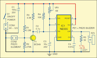
Fig. 1: Circuit of the glass break alarm

Circuit and working
  
Fig. 1 shows the circuit diagram of the glass break alarm. It is built around a piezo element connected across connector CON2, transistor BC549 (T1), timer NE555 (IC1), a piezo buzzer (PZ1) and a few other components.
A small piezo element used in the piezo buzzer is used as a sensor. It may be fixed at the centre of the window glass. IC1 is wired in monostable multivibrator mode, which is triggered by the piezo element. Output of IC1 is used to drive piezo buzzer PZ1. LED1 indicates the high-state output at pin 3 of IC1. Time delay can be adjusted by potentiometer VR1. Use an ordinary piezo buzzer at the output to generate a warning sound. This circuit works on 9V-12V DC.

When an intruder tries to break the glass, the piezo element generates an electric pulse, which is amplified and sent to the monostable multi-vibrator (IC1). The high output of IC1 drives LED1 and also produces a sound to indicate that someone is breaking the glass.

The 9V-12V DC power supply is connected across CON1, and the piezo element is connected across connector CON2.

Construction and testing
An actual-size, single-side PCB for the glass break alarm is shown in Fig. 2 and its component layout in Fig. 3. Enclose the PCB in a suitable small box in such a way that the piezo buzzer sounds when someone tries to break the glass window. Fix the piezo element at the centre of the window glass for best results.

Fig. 2: Actual-size PCB of the glass break alarm

Fig. 3: Component layout of the PCB


Use of 8-pin IC base is recommended for IC NE555.
Read More
WEARIFY

Simple Over Voltage Protector Circuit Diagram

This is the Simple Over Voltage Protector Circuit Diagram. The whole circuit of over voltage protector is build and fabricated around operational amplifier used as comparator. The inverting input is given to pin 2 of op-amp IC (IC1) with reference voltage of 5.1V from zener diode. Similarly, non-inverting input is given to pin no 3 of IC1 use as sensor for over voltage protector for sensing voltage fluctuation in the mains. The two transistors T1 and T2 conduct alternating (i.e. one at a time) according to the voltage of mains.

Simple Over Voltage Protector Circuit Diagram

Simple Over Voltage Protector Circuit Diagram


When voltage is around or below 240V AC transistor T1 is in off-state where T2 energized relay RL1. Similarly, when voltage becomes beyond 240V (i.e. above 240V) T1 is in conducting-stage and T2 is in off-stage which de-energized the relay RL1 and switch-off the appliance.

PARTS LIST

Resistors (all ¼-watt, ~+mn~ 5% Carbon)

R1 = 147 Ω/2W

R2 = 100 Ω/1W

R3 = 330 Ω

R4 = 100 KΩ

R5 = 1.8 KΩ

R6, R7 = 1 KΩ

VR1 = 10 KΩ

VR2 = 22 KΩ
Capacitors

C1, C4, C5 = 0.01 µF

C2 = 1000 µF/25V

C3 = 100 µF/25V
Semiconductors

IC1 = µA741 (Operational Amplifier)

IC2 = 7812

T1= BC547

T2 = SL100

D1, D2, D3, D4, D5 = 1N4007

D6 = 1N4148

ZD1 = 5.1V zener diode
Miscellaneous

X1 = 230V AC primary to 7.5V-0-7.5V, 1A secondary transformer

RL1 = 12V, 200Ω 1 C/O Relay

LED1 = RED
Read More
WEARIFY

Automatic Dipper for Vehicles Project

While driving a car in night a problem like many drivers do not dip the head lamps of their vehicles in night while approaching. The several switching operation is used to dip the head light which may distract the concentration. To overcome this type of problem the innovative group Dreamlover Technology designs a unique electronics gadget called “Automatic Dipper” using very popular IC NE555 and LDR.

Circuit Description

The entire circuit of automatic dipper consist LDR followed by timer IC NE555 (IC1) and few other components, where LDR is used as sensor. LDR sense the light and change its internal resistance according light fall on it, which is further mounted in PVC pipe of 4 cm length positioned on the grill of car or in front such that the light fall on the LDR only when vehicles is approaching and is distance of 3M to 9M. When light fall on it the resistance decrease and makes output of IC1 low which energized the relay. The relay operates and voltage across the head lamps is reduced. When the distance between two approaching vehicles is more than 9 meter or less than 3 meter the circuit is not operated.

Automatic Dipper for Vehicles Circuit Diagram 

Automatic Dipper for Vehicles Project
 

The operating and non operating distance of the circuit can be varied by proper positioning of the PVC pipe and by adjusting the variable resistor VR1.


PARTS LIST
Resistors (all ¼-watt, ± 5% Carbon)

R1 = 10 Ω/10W

VR1 = 10 KΩ
Semiconductors

IC1 = NE555 (timer IC)

D1 = 1N4001
Miscellaneous

RL1 = 12V/100 Ω

LDR1= Light dependent resistor
Read More
WEARIFY

Electronic siren circuit Diagram

This is a compact electronic siren circuit based on three transistors.This circuit is suitable for in corporating with other alarm or siren projects such as burglar alarms, automatic factory sirens etc or a simple push to on alarm.

The  electronic siren circuit given here  is  based on a complementary transistor pair consisting of Q2 & Q3 (BC557 & BC 37)  wired as an astable multivibrator oscillator,which directly drives the speaker.The transistor Q1 is used to provide a full charge on capacitor C2 when power is turned ON. When push button switch S1 is pressed , the capacitor C2 slowly discharges through resistor R8.This makes the circuit to  oscillate at a low frequency that increases to a high frequency and kept indefinitely as the capacitor is fully discharged. When the switch P1 is released, the output  frequency decreases slowly as C2 is charged to the  positive voltage through resistance R6 and the Base-Emitter junction of tramsistor Q2. When C2 is fully charged to the positive battery voltage the  circuit stops oscillating.

Electronic siren circuit Diagram with Parts list.

Electronic siren circuit Diagram


Notes.


  • A 12 V battery or a a well regulated 12V DC power supply can be used to power the circuit.
  • Assemble the circuit on a good quality PCB or common board.
  • The switch S1 can be used to activate the alarm.
  • The switch S2 can be used as a power switch.
  • You can experiment on the tone of alarm by using different values for C2 and R8.
Read More
WEARIFY

Solar Powered SLA Battery Maintenance Schematic

This circuit was designed to ‘baby-sit’ SLA (sealed lead-acid or ‘gel’) batteries using freely available solar power. SLA batteries suffer from relatively high internal energy loss which is not normally a problem until you go on holidays and disconnect them from their trickle current charger. In some cases, the absence of trickle charging current may cause SLA batteries to go completely flat within a few weeks. The circuit shown here is intended to prevent this from happening. Two 3-volt solar panels, each shunted by a diode to bypass them when no electricity is generated, power a MAX762 step-up voltage converter IC.

Solar Powered SLA Battery Maintenance Circuit Diagram:

Solar Powered SLA Battery Maintenance Schematic

The ‘762 is the 15-volt-out version of the perhaps more familiar MAX761 (12 V out) and is used here to boost 6 V to 15 V.C1 and C2 are decoupling capacitors that suppress high and low frequency spurious components produced by the switch-mode regulator IC. Using Schottky diode D3, energy is stored in inductor L1 in the form of a magnetic field. When pin 7 of IC1 is open-circuited by the internal switching signal, the stored energy is diverted to the 15-volt output of the circuit. The V+ (sense) input of the MAX762, pin 8, is used to maintain the output voltage at 15 V. C4 and C5 serve to keep the ripple on the output voltage as small as possible. R1, LED D4 and pushbutton S1 allow you to check the presence of the 15-V output voltage.

D5 and D6 reduce the 15-volts to about 13.6 V which is a frequently quoted nominal standby trickle charging voltage for SLA batteries. This corresponds well with the IC’s maximum, internally limited, output current of about 120 mA. The value of inductor L1 is not critical — 22 µH or 47 µH will also work fine. The coil has to be rated at 1 A though in view of the peak current through it. The switching frequency is about 300 kHz. A suggestion for a practical coil is type M from the WEPD series supplied by Würth (www.we-online.com). Remarkably, Würth supply one-off inductors to individual customers. At the time of writing, it was possible, under certain conditions, to obtain samples, or order small quantities, of the MAX762 IC through the Maxim website at www.maxim-ic.com.
Read More
WEARIFY

Micro Inverter circuit DC voltage AC 12v x110v


This is a micro-inverter DC voltage to AC from a 12v battery can generate a voltage of 110 or 220 volts AC and a frequency of 50Hz to 60Hz.

Micro Inverter circuit DC voltage AC 12v x110v Circuit Diagram:

Micro Inverter circuit DC voltage AC 12v x110v


The circuit is very simple and does not need a printed circuit board, It is composed of two transistors oscillators that generate the square wave pulse to the transformer in the case is 10 +10 and its output 220V or 110V. This circuit is 50Hz, but can be changed by changing the value of RC .


This circuit has the power transistor and that depends on the transformer.

Micro Inverter circuit DC voltage AC 12v x110v

Read More